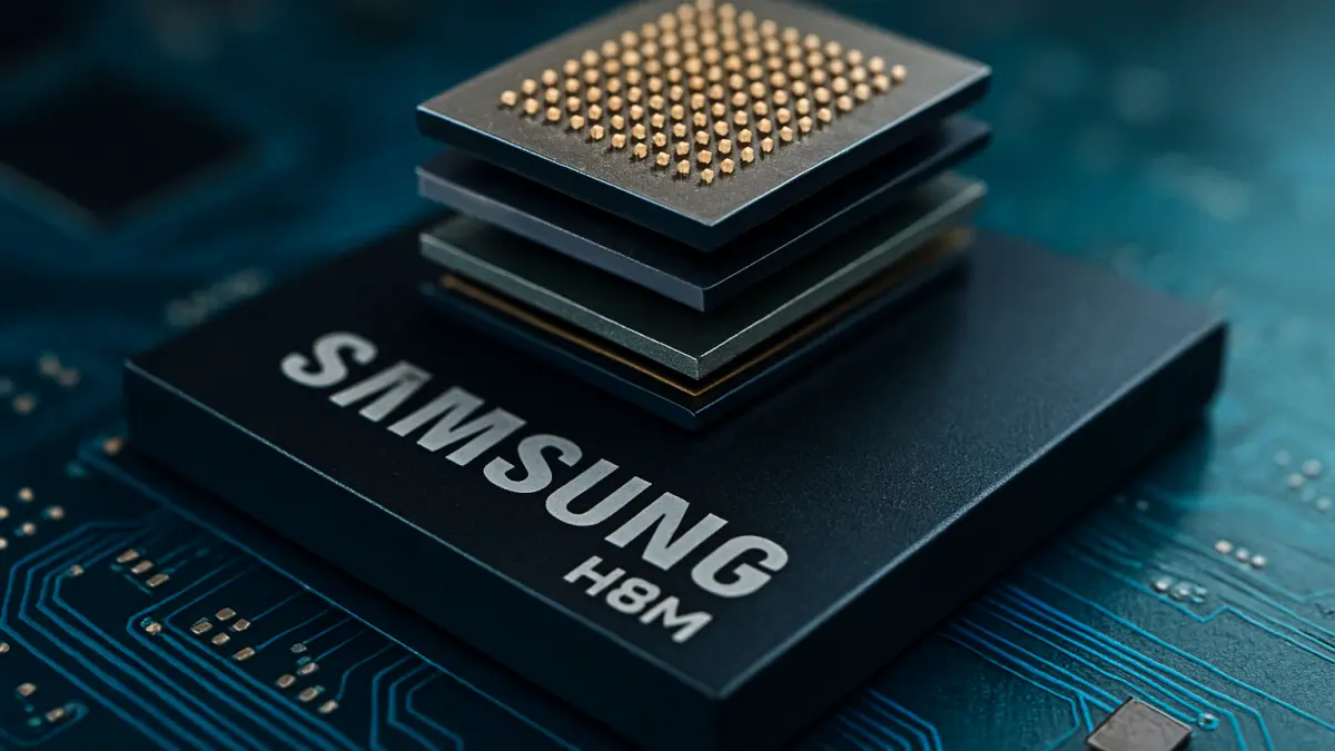

Samsung has revealed an ambitious three-phase roadmap for High Bandwidth Memory (HBM) at Hot Chips 2026, outlining a progressive integration of logic and compute capabilities directly into memory stacks. The plan culminates in zHBM, a design that stacks DRAM directly on top of the processor, aiming to dramatically boost performance and efficiency.
This development matters because it challenges the traditional separation between memory and logic chips, which has long been a bottleneck in computing speed and power consumption. By embedding logic into the base die of HBM and eventually stacking DRAM on the processor, Samsung is targeting lower latency and higher bandwidth, critical for AI, high-performance computing, and advanced graphics workloads.
The broader semiconductor industry has been exploring tighter integration of memory and logic, with approaches like chiplets and 3D stacking gaining traction. Samsung’s roadmap signals a clear strategic push to lead this space by evolving HBM beyond a passive memory component into an active compute element. This could reshape how future chips are architected, potentially reducing the need for separate memory controllers and improving data throughput.
Strategically, Samsung’s phased approach allows for incremental adoption and refinement, starting with logic integration in the base die before moving to full DRAM-on-processor stacking. This roadmap may influence competitors and ecosystem partners to accelerate their own memory-logic convergence efforts, impacting supply chains and design methodologies.
What to watch next is how quickly Samsung can move from roadmap to production and how the industry responds. Adoption by major CPU and GPU vendors will be key, as will the real-world performance gains and power efficiencies realized. Samsung’s vision could redefine memory hierarchy and chip design in the coming years.