
Elon Musk’s proposed Terafab semiconductor project could become one of the most ambitious chip manufacturing initiatives in the world, with Tesla and SpaceX aiming to establish a large-scale production operation capable of manufacturing up to one million semiconductor wafers per month by 2032. First announced in March 2026, the initiative reflects Musk’s growing concern about the availability of advanced chips needed to support artificial intelligence, autonomous vehicles, robotics, and space infrastructure.
The proposed manufacturing capacity includes approximately 700,000 wafers per month dedicated to memory production, with the remainder allocated to logic chips. If achieved, that scale would place Terafab among the industry’s largest semiconductor manufacturing operations. However, building a competitive fabrication operation requires years of engineering, substantial capital investment, specialized equipment, and access to an increasingly complex global supply chain.
Why Tesla and SpaceX Want Their Own Semiconductor Supply
Tesla’s demand for computing hardware has expanded beyond the processors used in electric vehicles. Its autonomous driving systems, humanoid robotics programs, and AI training infrastructure require increasingly sophisticated chips. SpaceX also depends on specialized electronics for spacecraft, satellite communications, and ground-based infrastructure, while xAI’s development of large artificial intelligence models creates additional demand for high-performance accelerators and memory.
These requirements expose Musk’s companies to the same semiconductor supply constraints affecting major technology firms worldwide. Today, designing a chip and manufacturing it are fundamentally different operations. Companies can develop custom processors while relying on specialized foundries such as TSMC or Samsung to fabricate them. Terafab represents an attempt to bring more of that manufacturing process under direct control.
In principle, vertical integration could allow Tesla and SpaceX to coordinate chip design, manufacturing priorities, and hardware development schedules more closely while reducing exposure to external production bottlenecks. However, owning a fabrication facility does not automatically guarantee lower costs or faster innovation. Those benefits depend on manufacturing efficiency, technological competitiveness, and the ability to sustain high production yields.
One Million Wafers Per Month: Understanding the Scale
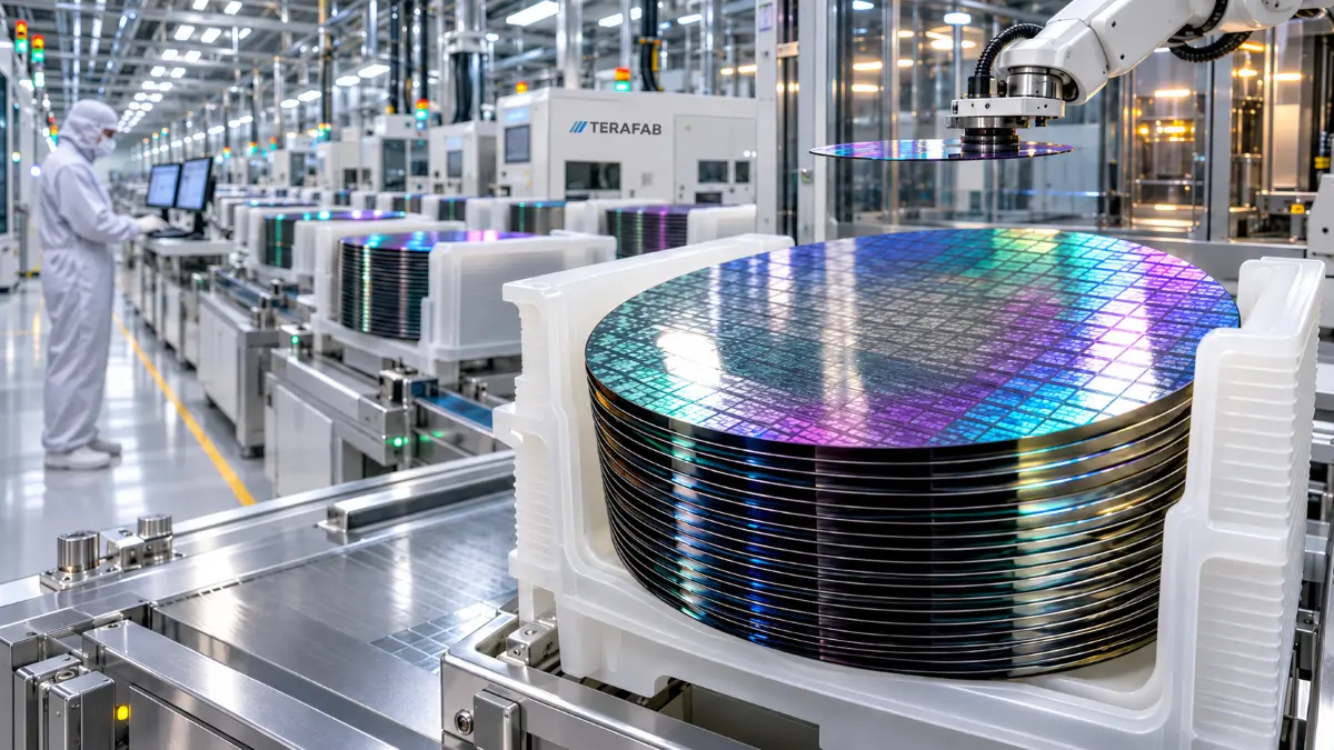
Terafab’s stated target of one million wafers per month is extraordinary for a new semiconductor manufacturing operation. A semiconductor wafer is a circular silicon substrate on which numerous integrated circuits are fabricated through a sequence of highly controlled manufacturing steps. The number of usable chips produced from each wafer depends on several factors, including wafer diameter, chip size, manufacturing technology, and defect rates.
A large AI processor may occupy considerably more silicon area than a compact automotive controller, meaning the same wafer capacity can translate into very different numbers of finished chips. The proposed allocation of approximately 700,000 wafers per month to memory production is particularly significant, given the growing importance of memory bandwidth and capacity in modern AI systems.
High-bandwidth memory (HBM) has become a critical component in advanced AI accelerators, while conventional DRAM remains essential for servers and other computing infrastructure. However, manufacturing memory chips at scale requires specialized process technologies and extensive production expertise. Advanced memory products can also require sophisticated packaging and integration techniques. Terafab’s proposed wafer capacity should therefore be understood as a long-term production ambition, not evidence that the project has already secured the technologies or infrastructure necessary to achieve it.
The Challenge of Building Both Logic and Memory Chips
One of the project’s most difficult engineering challenges is its apparent ambition to manufacture multiple semiconductor categories. Logic chips, including processors and AI accelerators, are generally optimized for computational performance, power efficiency, and transistor density. Memory chips prioritize storing and retrieving information efficiently, often using manufacturing structures and processes that differ substantially from those used for advanced logic.
Producing both categories competitively would require significant investment in fabrication equipment, process development, testing infrastructure, and engineering expertise. Modern semiconductor manufacturing involves hundreds of processing steps, including lithography, deposition, etching, implantation, and inspection. Advanced fabrication also depends on specialized equipment supplied by a relatively small number of global manufacturers.
Even after a production line becomes operational, manufacturers must improve yield, the percentage of usable chips produced from each wafer. Low yields can dramatically increase manufacturing costs, particularly when producing large, complex processors. For Terafab, reaching its stated wafer capacity would be only one measure of success. Achieving competitive yields, performance, reliability, and cost per chip would be equally important.
Space Applications Introduce Additional Requirements
SpaceX’s involvement adds another dimension to the initiative. Semiconductors used in spacecraft and satellites must withstand environmental conditions that differ significantly from those experienced by consumer electronics. Radiation exposure, temperature extremes, and long operating lifetimes can introduce additional reliability requirements.
Some space applications require radiation-hardened components, while others use commercially available chips combined with system-level protection and redundancy. Producing components suitable for these environments involves additional testing, qualification, and design considerations. A manufacturing operation serving both automotive and aerospace applications would therefore need to accommodate different performance, safety, and reliability standards.
Could Terafab Challenge Established Chipmakers?
The project’s scale invites comparisons with major semiconductor manufacturers, including Samsung, TSMC, and Micron. However, wafer output alone is not sufficient to establish competitive equivalence. A mature fabrication company operates multiple production lines, maintains established manufacturing processes, and benefits from years of accumulated engineering knowledge.
Advanced semiconductor manufacturing also requires continuous investment. A fabrication facility that is competitive when construction begins may need substantial upgrades before reaching full production. Terafab would face these challenges while established manufacturers continue developing newer process technologies.
Its competitive impact would also depend on whether production is primarily reserved for Musk’s companies or eventually offered to external customers. If most output is consumed internally, Terafab could become a major captive semiconductor operation without necessarily competing directly with commercial foundries for third-party business. That distinction matters when assessing its potential influence on industry pricing, manufacturing capacity, and supplier relationships.
What Must Happen Before 2032?
Reaching the proposed production target would require several major milestones. The project would need to secure suitable manufacturing sites, reliable electricity and water supplies, specialized equipment, materials, and an experienced engineering workforce. Semiconductor fabrication facilities also require extensive cleanroom infrastructure and highly controlled environmental conditions.
Equipment installation and process qualification can take considerable time, even after construction is completed. Terafab would then need to demonstrate successful pilot production, improve manufacturing yields, and gradually increase output toward its intended capacity.
The project’s capital requirements could be substantial. Leading-edge semiconductor fabrication facilities frequently require investments measured in tens of billions of dollars, and Terafab’s proposed scale could demand significantly more depending on its manufacturing technologies and development strategy. Until detailed construction schedules, equipment agreements, process technologies, and verified production milestones become available, the 2032 target remains an ambitious projection rather than an established manufacturing forecast.
A Long-Term Bet on Semiconductor Independence
Terafab illustrates a broader shift in how major technology companies view semiconductor manufacturing. As artificial intelligence becomes increasingly central to vehicles, robotics, cloud infrastructure, and autonomous systems, access to computing hardware is becoming a strategic consideration rather than simply a purchasing decision.
For Tesla and SpaceX, bringing chip manufacturing closer to their operations could provide greater influence over product development and long-term supply planning. Yet semiconductor manufacturing is fundamentally different from designing software, vehicles, or launch systems. Success requires sustained investment, specialized expertise, and manufacturing precision at an extraordinary scale.
Terafab’s defining achievement would not simply be producing one million wafers per month. It would be proving that a new entrant can build a reliable, economically competitive semiconductor manufacturing operation capable of supporting some of the world’s most demanding computing applications.