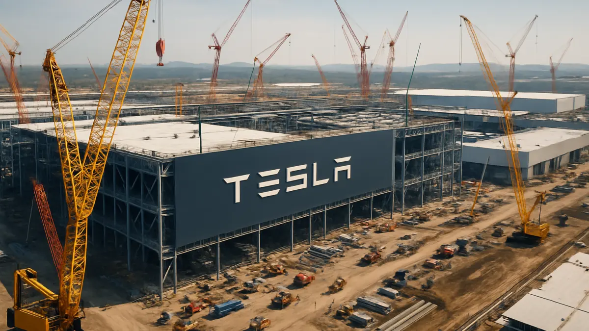

Elon Musk’s ambitious Terafab semiconductor facility has officially started to take shape, marking a significant expansion in chip manufacturing capacity. The project, backed by an initial $16.8 billion capital investment, is set to cover an enormous 100 million square feet, making it roughly three times larger than Samsung’s Pyeongtaek campus, one of the world’s largest semiconductor plants.
This massive buildout, driven by Musk’s SpaceX and Tesla, underscores a strategic push into semiconductor manufacturing amid ongoing global chip shortages and supply chain vulnerabilities. By controlling more of the chip production pipeline, Musk’s companies aim to reduce reliance on external suppliers and secure critical components for future electric vehicles, spacecraft, and other high-tech products.
The scale of Terafab signals a broader industry trend where tech giants are investing heavily in domestic chip production to regain manufacturing sovereignty. While Samsung, TSMC, and Intel have led the way with large fabs, Musk’s entry adds a new contender with a facility that dwarfs many existing sites. The $16.8 billion investment reflects both the high capital intensity of semiconductor fabrication and the strategic importance of chipmaking in the next decade.
Strategically, Terafab could reshape supply dynamics by increasing competition and capacity in the semiconductor sector. For Tesla and SpaceX, it promises greater control over supply chains and potential cost advantages. However, the project’s success will depend on navigating complex fabrication technology, workforce development, and market demand. The timeline and specific chip technologies planned for Terafab remain unconfirmed.
Industry watchers should monitor how Terafab progresses through construction and whether it can meet ambitious scale and technological goals. Its development will also offer insights into how non-traditional players like Musk’s companies influence semiconductor manufacturing’s future landscape.