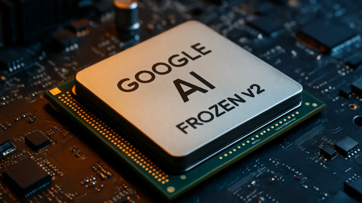

Google is reportedly working on a new server chip, dubbed Frozen v2, that integrates the architecture of its Gemini AI model directly into the silicon. This development aims to deliver a significant leap in efficiency, with engineers projecting the chip could process six to ten times more tokens per watt compared to the company’s latest TPU offerings.
The Frozen v2 chip represents a strategic move by Google to optimize hardware specifically for next-generation AI workloads. By etching Gemini’s architecture into the chip itself, Google could reduce latency and power consumption while improving throughput for large language models and other AI applications. This approach contrasts with traditional TPU designs that rely more heavily on software optimization and general-purpose hardware.
In the broader context, the Frozen v2 chip reflects an industry trend toward tighter integration between AI models and hardware. As AI workloads grow increasingly complex and power-hungry, companies like Google are seeking ways to push efficiency boundaries beyond incremental gains. Embedding model architecture directly into silicon could become a key differentiator in the race to build more powerful and energy-efficient AI infrastructure.
Strategically, this development could bolster Google’s competitiveness in cloud AI services and custom AI hardware markets. If successful, Frozen v2 might enable Google to offer faster and more cost-effective AI processing, attracting enterprise customers and researchers alike. However, details remain unconfirmed, and it’s unclear when Google plans to release the chip or how broadly it will be deployed.
What to watch next is how Frozen v2 performs in real-world AI tasks and whether this architectural embedding approach influences competitors’ chip designs. The chip’s efficiency claims, if validated, could set new standards for AI hardware performance and reshape expectations for AI infrastructure development.